Are you wondering about how to design a PCB? Printed Circuit Board (PCB) design is a crucial skill in the electronics industry.
Whether you’re a hobbyist looking to build a simple circuit or an engineer working on complex systems, understanding PCB design is essential. From the schematic design to the layout and component placement, the process requires a deep understanding of both electronics and design principles.
This guide will help you navigate through the core aspects of PCB design—from understanding its features and processes to learning about design tools, free resources, and practical examples.
Whether you’re a beginner or an advanced user, you’ll find valuable insights on how to design your own PCBs and start creating professional-quality boards.
What is a Printed Circuit Board
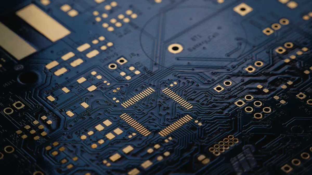
A printed circuit board (PCB) is the base of most electronics. It holds and connects parts like resistors, capacitors, and microchips. These parts are attached to the board, and copper lines link them. This setup creates a working circuit. Without PCBs, modern devices wouldn’t be small or efficient.
PCBs are used everywhere. They power phones, computers, and home gadgets. Cars use them for navigation and safety systems. Electric and self-driving cars also need PCBs to work well. As technology improves, smaller and better PCBs are in high demand.
Here’s a quick look at PCB market stats:
| Statistic | Value |
|---|---|
| Market Size in 2024 | USD 73.1 Billion |
| Market Forecast in 2033 | USD 97.7 Billion |
| Market Growth Rate 2025-2033 | 3.30% |
| Domestic Electronics Production FY23 | $101 billion |
| Mobile Phones Segment | 43% |
| Consumer Electronics Segment | 12% |
| Industrial Electronics Segment | 12% |
| Auto Electronics Segment | 8% |
| Electronic Components Segment | 11% |
More people are buying smartphones, tablets, and laptops. This increases the need for smaller, smarter PCBs. Car and factory tech also use PCBs for advanced systems. This shows how important PCBs are for future technology.
By learning about PCBs, you’ll see how they power devices. From simple tools to complex machines, PCBs are essential.
All Basics About PCB Design
PCB design means planning how a circuit board works. It involves placing parts and linking them with copper lines. This setup makes the parts work together in devices. Special software helps create these designs with precision.
The process starts with a diagram called a schematic. This shows how parts connect. Then, the schematic is turned into a physical design. Designers think about size, shape, and how well it works. Basics include layers, traces, and vias, which make circuits reliable.
Importance of PCB Design in Electronics
PCB design is key to making devices work well. A good design ensures parts work together without problems. Bad designs can cause overheating, signal issues, or device failure.
For wearable tech, PCB design affects size, flexibility, and materials. Designers must think about heat and moisture to make durable boards. Flexible devices need strong copper lines that won’t break. Materials also impact battery life and performance. Electrical and mechanical teams must work together for the best results.
By focusing on these details, designers make PCBs for modern devices like phones and medical tools.
Applications of Printed Circuit Boards in Everyday Devices
PCBs are in many gadgets you use daily. In phones, they link processors, memory, and sensors for smooth use. Laptops and tablets use PCBs to handle data and storage.
At home, appliances like fridges and washing machines use PCBs to work. Cars rely on PCBs for navigation, safety, and engine control. Electric and self-driving cars need advanced PCBs for tough tasks.
Wearables like fitness trackers need tiny, flexible PCBs. These designs must be small, strong, and long-lasting. As tech improves, PCBs help make devices smarter and more efficient.
Key Aspects of PCB Design
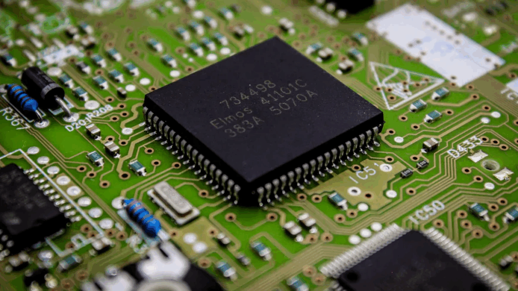
1. Layers (Copper, Substrate, Solder Mask, Silkscreen)
PCB layers are the building blocks of a circuit board. Each layer has a specific job to make the board work. The copper layer moves electrical signals between parts. The substrate gives the board its strength and shape. The solder mask keeps copper safe from rust and stops soldering mistakes. The silkscreen adds labels to help with assembly and repairs. These layers work together to create a strong and reliable PCB.
2. Traces and Pads
Traces and pads are key parts of a PCB. Traces are thin lines that carry signals between parts. Pads are spots where parts are attached with solder. The size and spacing of traces must be correct to avoid overheating or signal problems. Pads also need to fit parts properly to prevent soldering issues.
3. Vias and Ground Planes
Vias are tiny holes that connect different PCB layers. They come in types like through-hole, blind, and buried vias, each for specific uses. Ground planes are large copper areas that act as a shared electrical base. They help reduce noise and improve signal quality, which is important for high-tech PCBs.
Features of PCB Design
When learning about PCB design, you’ll find many features that make it important for today’s electronics. These features help circuit boards work well and fit different uses. Let’s look at the main points of PCB design.

- Compact and Lightweight Design
A PCB combines many parts into one small board. This makes devices smaller and lighter. For example, phones and wearables stay easy to carry because of this feature. - High Reliability
PCBs are made to work well for a long time. Strong materials and careful production keep circuits steady, even in tough conditions. This makes them great for medical tools and space systems. - Ease of Assembly and Maintenance
Good PCB designs make building and fixing easier. Parts are placed in order, so manufacturers can assemble them quickly. The silkscreen layer has labels to help with repairs or upgrades. - Cost-Effectiveness
PCBs save money for small and big projects. Machines do most of the work, cutting labor costs. Materials are used wisely, keeping waste low. This makes PCBs affordable for many industries. - Enhanced Signal Integrity
PCB design keeps signals clear and steady. Ground planes and good trace paths lower noise and interference. This helps devices work well, even in fast or sensitive tasks. - Customization Options
PCBs can be made to fit your needs. You can choose a simple board for basic gadgets or a multi-layer one for complex devices. This lets designers create new and exciting electronics.
Note: Knowing these features helps you see why PCB design is key to making strong and useful devices.
By focusing on these features, you can design PCBs that meet needs and improve how devices work.
Design Rules and Guidelines of PCD
Clearance and Creepage
Clearance and creepage are important for safe PCB designs. Clearance is the shortest air gap between two conductive parts. Creepage is the shortest path along the board’s surface. For example, circuits with 240VAC power need over 3mm of creepage. Following these rules prevents electrical problems and meets safety standards.
| Voltage line-to-neutral a.c. r.m.s. or d.c. | Clearance Values | Creepage Distance Values |
|---|---|---|
| ≤150 | 0.5 mm | 0.5 mm |
| >150≤300 | 1.5 mm | 1.5 mm |
Via Design Considerations
When designing vias, think about their size, location, and type. Smaller vias save space but cost more to make. Blind and buried vias are great for multi-layer PCBs because they connect specific layers without going through the whole board. Good via design helps signals flow smoothly and avoids manufacturing problems.
Signal Integrity and EMI Reduction
Keeping signals clear is vital for a working PCB. Shorter traces, smooth angles, and ground planes help maintain signal quality. To reduce noise, use shielding and place parts carefully. These steps make sure your PCB works well in modern devices.
Tip: Set design rules for trace sizes, spacing, and other details before starting. This helps avoid mistakes and ensures your PCB meets manufacturing standards.
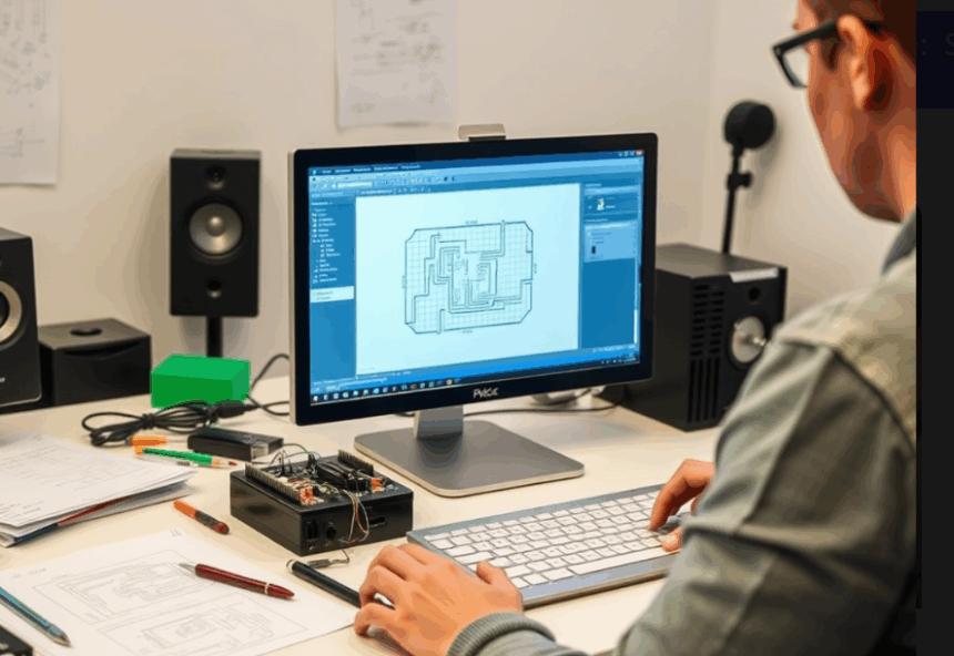
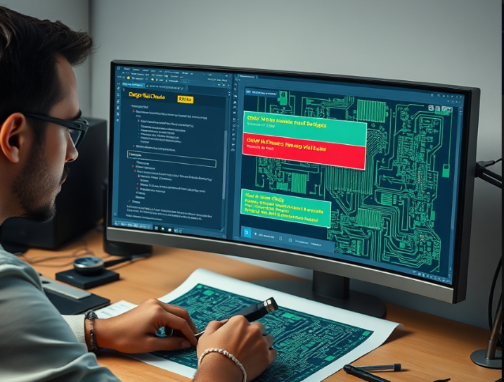
How to Design a PCB: Step By Step Guide for Beginners
Making a PCB involves steps to turn ideas into working boards. Follow these steps to design a reliable and efficient layout.
Step 1: Schematic Capture
Start by drawing a schematic diagram. This shows how parts connect in your circuit. Use software like KiCad or EasyEDA to make this easier. The schematic helps plan connections and ensures the circuit works.

Be accurate when drawing the schematic. Label each part clearly and check connections twice. Use symbols for parts like resistors, capacitors, and chips. This makes the diagram simple to understand. Review the schematic carefully to fix mistakes before moving on.
Tip: Software tools have libraries of symbols to help organize your circuit.
Step 2: Component Placement
Next, place the parts on the PCB layout. This step affects how well the board works and how easy it is to make.

Here are tips for placing parts:
- Align pin 1 of chips with the board’s direction. This reduces errors and speeds up assembly.
- Put power-hungry parts near edges or vents to avoid overheating. Bad placement can cause parts to fail early.
- Group similar parts together and keep signal paths short. This improves reliability and routing.
Think about the size of your design. If the PCB goes in a small device, save space by arranging parts tightly. Keep noisy parts away from sensitive ones to avoid interference. Good placement makes routing easier and keeps the layout clean.
Step 3: Routing
Routing connects parts using copper lines. This step turns your schematic into a physical PCB layout. Plan carefully to keep signals clear and avoid problems.

Manual Routing vs. Auto-Routing
You can route traces by hand or use auto-routing tools. Manual routing gives better control and performance but takes more time. Auto-routing is faster but may need adjustments for efficiency.
Optimizing Trace Width and Length
Trace width and length affect how the PCB works. Wider traces carry more current, while shorter ones reduce delays. Use calculators to pick the right width for your circuit.
Avoid sharp angles in traces. Use smooth curves or 45-degree angles instead. Keep fast signal traces short for better quality. Use vias to connect layers if your design has multiple levels.
Note: Follow your manufacturer’s rules for trace width, spacing, and via size.
By following these steps, you can design a neat and functional PCB. Each step builds on the last, making the process smooth and effective.
Step 4: Design Rule Checks (DRC)
Design Rule Checks (DRC) make sure your PCB design follows manufacturing rules. This step checks things like trace width, spacing, and via size. Running a DRC helps find mistakes early, saving time and money during production.
Here’s why DRC is important:
- It boosts manufacturing success by matching your design to production needs.
- It lowers failure chances by spotting problems in key areas like power lines.
- It improves product quality by fixing design issues before production starts.
| Benefit | Description |
|---|---|
| Better manufacturing success | DRC ensures designs fit production rules, cutting defects. |
| Lower failure chances | Finds problems in critical areas, reducing risks of errors. |
| Higher product quality | Fixes design flaws early, ensuring better performance and satisfaction. |
Tip: After running the DRC, always review your design one last time. This helps catch any missed errors and ensures your PCB is ready for production.
Step 5: Preparing for Manufacturing
After passing the DRC, the next step is getting your design ready for production. This includes creating important files and organizing everything for smooth PCB manufacturing.

Making Gerber Files
Gerber files are what manufacturers use to build PCBs. These files show details about each layer, like copper lines, solder masks, and labels. To create Gerber files:
- Use your design software to export the layout as Gerber files.
- Check the files to make sure they match your design.
- Add a drill file for holes and vias, which manufacturers need for drilling.
Note: Tools like KiCad or EasyEDA make it simple to create Gerber files with built-in features.
Panelization and BOM Creation
Panelization means placing multiple PCB designs on one panel. This saves materials and speeds up production. Manufacturers like this because it makes their work easier.
A Bill of Materials (BOM) lists all the parts needed for your PCB. It includes details like part numbers and quantities. To make a BOM:
- Use your software to export a list of parts.
- Double-check the list for accuracy.
- Share the BOM with your manufacturer to ensure correct parts are used.
Good preparation improves production results. For example:
| Metric | Improvement Observed |
|---|---|
| Faster Production | Over 30% increase in efficiency |
| On-time Delivery | At least 98% success rate |
| Cost Savings | 15%-20% reduction in production costs |
| Higher Yield Rates | Up to 95% improvement in output quality |
| Better Customer Satisfaction | Consistent quality and timely delivery |
By following these steps, you’ll make sure your PCB is ready for production. This preparation saves time and ensures a high-quality final product.
Online PCB Design Software & Tools
Picking the right PCB software is important for good designs. Whether you’re new or experienced, there are many tools to try. Below is a list of free and paid options with key features to help you decide.
Free Software Options
KiCad: Free tool for schematics and PCB layouts
URL:https://www.kicad.org/

KiCad is open-source software with tools for PCB design. It includes schematic drawing, layout editing, and a 3D viewer. This makes it great for students and hobbyists. Its active community offers guides and help, making it beginner-friendly.
EasyEDA: Online tool with built-in parts libraries
URL: https://easyeda.com/
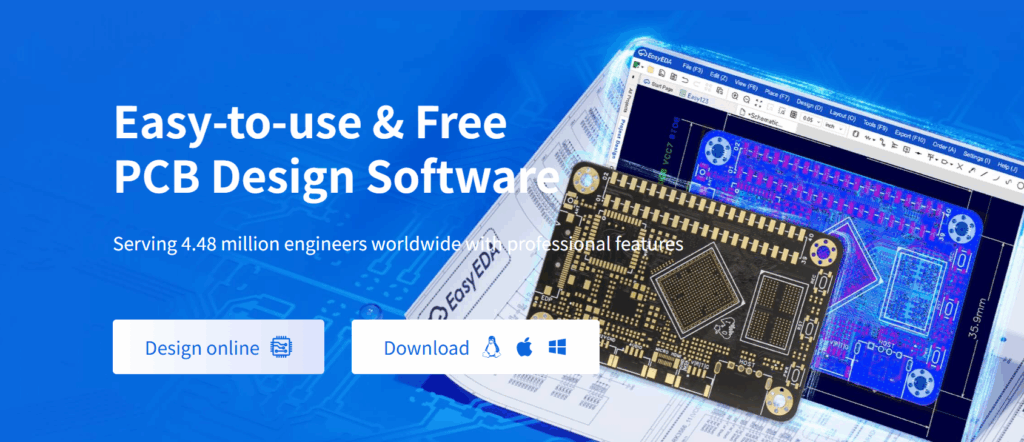
EasyEDA is a web-based PCB design tool. You can create schematics and layouts directly in your browser. It has a large library of parts and supports teamwork. This makes it perfect for small groups working on simple projects.
Fritzing: Easy software for beginners
URL:https://fritzing.org/
Fritzing is ideal for those just starting with PCB design. Its drag-and-drop feature makes creating layouts simple. You can design basic circuits and test them easily. Teachers and makers love it for its focus on learning.
Tip: Free tools are great for learning and small projects. They let you practice PCB design without spending money.
Paid Software Options
Altium Designer: Advanced tool for professionals

Altium Designer is a top choice for complex PCB projects. It offers fast routing, multi-board design, and team collaboration. It’s best for big teams working on detailed designs.
Eagle: Popular software with a free version
Eagle is well-known in the PCB world. It has an easy interface and strong part libraries. The free version works for small projects, while the paid version adds features like auto-routing and simulations.
OrCAD: High-end software for detailed designs
OrCAD is made for engineers needing precise layouts. It excels in testing and analysis, ensuring high-quality designs. Its large library and simple interface make it a favorite for professionals.
Note: Paid tools often have advanced features and better support. They are worth it for big or complex projects.
Key Features to Look for in PCB Software
- Easy-to-Use Interface: A simple interface is important, especially for beginners. Choose software that is easy to learn and use.
- Good Library Management: A strong library gives you access to many parts. This saves time and ensures accurate designs with verified components.
- Testing and Analysis Tools: Testing tools let you check your design before making it. They help find problems and improve reliability. Analysis tools also improve signal quality and reduce noise.
Did you know? The PCB software market is growing fast, with a 13.4% yearly increase expected from 2024 to 2031. This shows the rising need for advanced tools to handle complex designs.
By knowing the features and options, you can pick the best PCB software. Free tools are great for learning, while paid ones help with advanced projects. The right software will make your designs better and easier to create.
Tips for Beginners to Design a PCB Board
Keep Schematics and Layout Aligned
Making sure schematics match the layout is very important. It keeps your diagram and physical design consistent. Real-time updates help avoid mistakes like wrong connections or missing parts. These errors can cause problems during use or manufacturing.
Why alignment matters:
- Updates in real-time stop outdated or mismatched designs.
- Teams work better with the latest shared design files.
- Using standard libraries avoids picking duplicate parts, keeping quality high.
- Spotting issues early saves time and money before production.
- It keeps the original design idea intact and reliable.
By aligning schematics and layout, you simplify the process and reduce errors.
Add Ground Planes for Better Performance
Ground planes are key for making your PCB stable and reliable. They act as shields, cutting down on interference and keeping signals clear. This is especially useful for high-frequency or sensitive designs.
Why ground planes help:
- Continuous ground planes lower interference, which is great for flexible PCBs.
- Good grounding improves signal quality in rigid-flex PCBs, reducing noise and boosting stability.
Make sure your ground plane is connected and uninterrupted. This small step makes your PCB work much better.
Design for Easy Manufacturing
Designing with manufacturing in mind makes your PCB easier and cheaper to produce. Thinking about this early avoids delays and lowers costs.
Here’s how manufacturability helps:
| Improvement Metric | Benefit |
|---|---|
| Lower production costs | Fewer design changes and less wasted material. |
| Better product quality | Meets manufacturing rules for reliable performance. |
| Fewer production mistakes | Designs optimized for smooth manufacturing processes. |
| Faster time-to-market | Fixing issues early speeds up production. |
| Higher product reliability | Regular checks ensure better design compliance. |
| Improved first-pass success | Success rates rise from 85% to 98% in case studies. |
Follow guidelines like using common parts, proper trace widths, and correct spacing. This makes your PCB better and faster to produce.
Start with Simple Designs
When learning PCB design, begin with easy projects. Don’t start with complicated circuits or multi-layer boards. Instead, try single-sided PCBs. These have parts and traces on one side, making them simpler to handle. They are great for learning basic skills like layout, routing, and soldering.

Pick a small project, such as a blinking LED or simple power supply. These tasks help you practice placing parts and connecting them with traces. You’ll also learn to fix common problems, like broken connections or wrong placements. By mastering these basics, you’ll be ready for harder designs later.
Use free tools like KiCad or EasyEDA for your first projects. These programs are easy to use and include libraries of parts. They let you try different layouts without spending money. As you get better, you can move on to more advanced features, like multi-layer boards or complex routing.
Tip: Start with small, simple designs. Focus on learning, not perfection. Mistakes will help you improve.
Starting simple teaches you the basics of PCB design. It prepares you for creating more advanced circuits in the future.
Learn from Online Tutorials and Communities
Online tutorials and groups are great for learning PCB design. Tutorials guide you step-by-step on making schematics, placing parts, and routing traces. Websites like Coursera, Udemy, and edX offer courses for beginners and experts. These courses are flexible and affordable, letting you learn at your own speed. Many include quizzes and forums where you can ask questions and get help.
Joining online groups connects you with other PCB designers. Platforms like Reddit, Discord, and forums let you share your work and get feedback. You can also join design challenges or group projects to improve your skills. For example, you might create a small PCB for a wearable device as part of a challenge.
Did you know? Many designers say online groups helped them solve tough problems. Sharing ideas and asking questions can help you avoid mistakes and make better designs.
Using tutorials and joining communities speeds up your learning. They give you useful tips and support, making PCB design more fun and rewarding.
Online PCB Design Book | Free Printable PDF
How to Get the Free PDF
Getting the free PDF is easy and fast. Just find the “Download Free PDF” button in this blog section. Click it, and you’ll go to a secure page to save the file on your device.
Another option is signing up for our newsletter. Subscribers receive the PDF directly in their email. Plus, they receive updates with helpful PCB design tips and tools. This way, you’ll always have the newest resources handy.
Tip: Save the download page as a bookmark. This makes it simple to return and grab the resource whenever you need it.
What’s Inside the PDF
The free PDF is a complete guide to learning PCB design. It walks you through everything, from the basics to making your first PCB prototype. Here’s what it includes:
- Introduction to PCB Design: Understand how PCBs work and why they’re important.
- Step-by-Step Design Process: Follow clear steps to create a PCB, like drawing schematics, placing parts, and routing.
- Software Recommendations: Check out free and paid tools with advice on picking the best one.
- Prototyping Tips: Learn how to turn your design into a real PCB, including preparing files and working with manufacturers.
- Troubleshooting Guide: Find fixes for common problems to ensure your PCB works properly.
The guide also has diagrams, examples, and checklists to make learning simpler. Whether you’re just starting or improving your skills, this PDF has you covered.
Why Offline Learning Helps
Offline learning has many benefits, especially for tricky topics like PCB design. With the free PDF, you can learn at your own speed without needing the internet. This lets you focus better on each step without interruptions.
Printed or saved materials are great for taking notes and marking key points. You can keep the PDF open while working on your PCB project, so it’s always there when you need it.
Did you know? Research shows offline learning can boost memory by up to 25%. Reading from a document helps you understand and remember better than scrolling online.
By downloading the PDF, you’ll have a dependable guide you can use anytime. It’s perfect for beginners who want to learn PCB design step by step.
Examples & Ideas for PCB Design
PCB design lets you create cool and useful projects. Whether you’re just starting or already skilled, trying new ideas can help you learn more and make unique designs. Here are some fun examples to inspire you.
1. Make PCBs at Home
You can now make PCBs at home with simple tools. One method uses a 405nm laser and photoresist film. The laser draws tiny lines, as small as 0.2mm, on the PCB using UV light. This makes it easy for hobbyists to create custom boards without spending much money. It’s a great way to try out your own designs.
2. Use Eco-Friendly Materials
Eco-friendly PCBs are better for the planet. A new idea uses wood-based materials called lignocellulose nanofibrils (LCNFs) to make biodegradable boards. These boards are 70% eco-friendly and work well with 3D-printed cases. This reduces waste and helps create greener technology. You can try similar materials for your own projects.
3. Try Flexible PCBs
Flexible PCBs are great for gadgets like smartwatches and fitness bands. These boards can bend and twist without breaking. You can design circuits that fit unusual shapes, making them perfect for wearable devices. This is a fun way to create products for health, sports, or fashion.
4. Design LED Displays
LED PCBs are awesome for making bright displays. You can create boards that control LED grids to show patterns, animations, or text. These are perfect for decorations, ads, or art projects. With some creativity, you can make eye-catching designs.
5. Build IoT Devices
IoT devices need PCBs to work. You can design a board for a smart home gadget like a temperature sensor or security camera. These projects teach you how to connect sensors, microcontrollers, and wireless parts in a small space.
Tip: Start with easy projects and slowly try harder ones. Testing different ideas will help you get better at PCB design.
By exploring these ideas, you can learn new skills and create PCBs that solve everyday problems.
Conclusion
You’ve learned the basics of PCB design, including its features, process, and software tools. The free PDF is a helpful offline guide to review what you’ve learned. With this information, you can start making your own PCB designs. Begin with easy projects, follow the tips shared, and try out the suggested tools. Every project will help you improve and get better at PCB design. Take the first step today and begin your learning journey!
For more resources, tutorials, and guides on PCB design, visit GES PCB and start your journey today!
FAQs on PCB Design
Q1. How do I get started with designing a simple PCB?
Start by learning basic electronics principles and use free PCB design tools like KiCad or EasyEDA. Then, move on to simple projects like designing an LED blink circuit.
Q2. How to learn schematics and circuit design?
The best way to learn is by studying schematics of simple circuits. Start with basic tutorials and build your understanding from there. There are free courses and YouTube tutorials to get started.
Q3. How to code an electronic circuit?
For microcontroller-based circuits, you will need to learn embedded programming using languages like C/C++ and platforms such as Arduino IDE.
Q4. Where can I learn PCB design online for free?
There are numerous free resources available online, including tutorials on KiCad, EasyEDA, and other PCB design platforms. You can also find free courses on platforms like Coursera and Udemy.
Q5. Is it possible to learn PCB design through self-study?
Yes, many PCB designers are self-taught. With resources like books, tutorials, and free design software, anyone can learn PCB design at their own pace.
Q6. Recommendations to a newbie wanting to learn PCB design?
Start with basic projects, use beginner-friendly design tools like EasyEDA and KiCad, and follow online tutorials. Don’t rush—practice designing simple boards first.
Q7. Guide to PCB design practice?
Focus on mastering the basics—learn how to create a schematic, place components, and route traces. As you gain experience, try designing more complex circuits, test your designs, and improve your skills with each project.